Fabrication mistakes on printed circuit boards (PCB) can happen, but this simple method can help you avoid compounding them in the process.
Increasing layer count means increasing complexity. Also, increasing layer count correlates with increasing importance of the layer order, thickness, and spacing. It is likely the additional layers were added to accommodate a more complicated design, so things like impedance control may be needed, requiring specific layer ordering, spacing, and copper weights.
More layers means more opportunity to swap a layer accidentally, potentially causing signal integrity issues, or even a non-functional design.
Auto-generated layer names are not always the best for determining overall order, either. A four-layer board is quite easy, as there are only so many combinations of Top, Ground, Power, and Bottom. The latest design I worked on had six layers (01_TOP, 02_GND, 03_Inner1, 04_Inner2, 05_PWR, 06_Bottom), which is still rather straightforward, especially considering the leading “0X” layer number that I added.
But bumping the layer count to eight or more becomes much more complicated. Once you have 24 layers, the stack-up possibilities are endless.
Mistakes happen. The most likely source of error I have encountered in inconsistent layer naming conventions, especially in auto-generated layer names.
As a test, I decided to add two layers to my above example. My chosen PCB tool (OrCAD in this case) did not prepend the “0X” layer number to my layer names. I added the layers to the middle of the board as new layers 4 and 5, but nothing is stopping me from sending a board package with (01_TOP, 02_GND, 03_Inner1, 04_Inner2, 05_PWR, 06_Bottom, GND2, PWR2) as the layer names. Good luck deciding where to put GND2 and PWR2. Are they layers 7 and 8? 4 and 5? These should be defined in a layer stack-up note, but what if it is missed?
As an additional example, I started a new project and added four internal layers. Unfortunately, I did not pay much attention when running the “add new layer” command and ended up with the following layer stack-up.
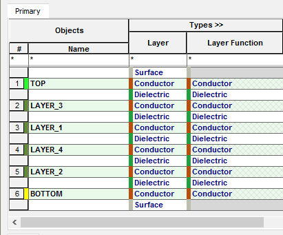
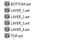
Compared to how Windows Explorer sorts layers based on the outputted Gerber files, which is correct?
I hope that it is clear by now that layer naming is important! Ideally, someone along the review process could notice the inconsistency. Again, mistakes do happen.
Visual inspection of the top and bottom layers is easy enough; they are on the top and the bottom. How do we ensure that the internal layers are correct? Perhaps you could cut a spare board using a band saw, but without pour-areas on signal layers, this would literally be hit-or-miss, as well as potentially expensive!
Confirming the artwork itself is not possible, short of some x-ray technology, but there is a very simple way to confirm layer ordering, copper thickness, and layer spacing.
A PCB stacking stripe is a region of unconnected, exposed copper of increasing length along a board’s edge meant for a visual reference of layer ordering.
The top layer is typically the shortest, with each additional layer increasing in length with each layer aligned along one side. This creates an easy visual stack-up; if it doesn’t look like a staircase then something is wrong!
There can also be an additional strip next to the aligned side on each layer to ensure proper layer alignment. Keep in mind that these shapes should overhang the board outline (to be sure the copper is exposed once the board is removed from the panel) and that the exposed copper is not internally connected. Make sure to use a dummy net, especially on power and ground planes.
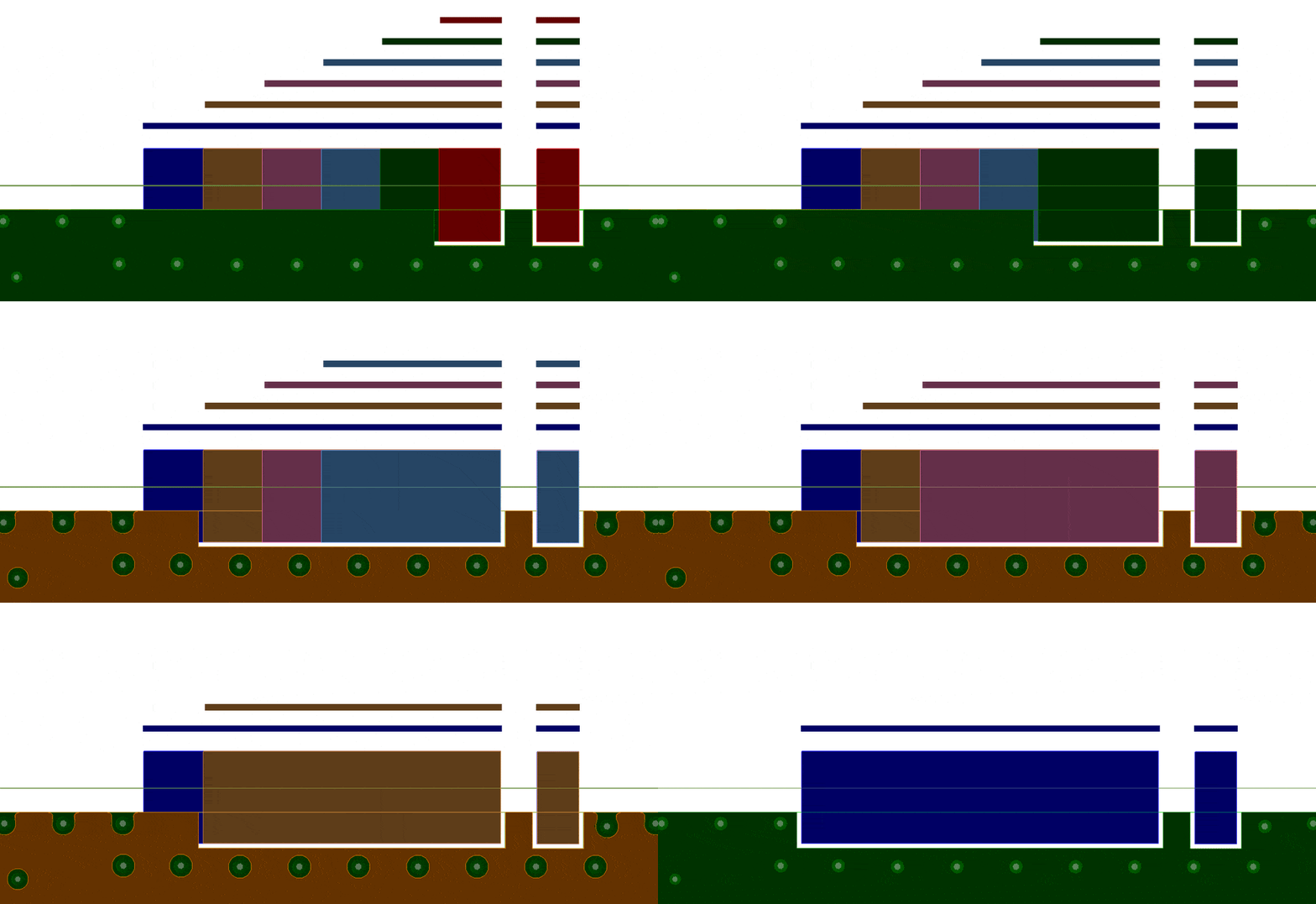
It should be quick and easy to cycle through each layer in your PCB software or Gerber viewer prior to sending files to a board manufacturer to ensure that each layer correctly ordered. If the copper shape does not grow incrementally with each additional layer, you know something is amiss.
Layer ordering is easy to confirm. If the board edge does not look like a staircase then something is wrong! Copper thickness and layer spacing are also easy to inspect by peeking at the board edge.
Given that a stacking stripe is simply a series of copper pour areas, there is no added component cost, and it is quite easy to implement, requiring very little overhead.
In order to prevent shorts, it is typically a considered a best practice to pull copper pours back from the board edge at least 25 mils. In this scenario, we want the copper to be exposed! As long as your copper is isolated, this exposed copper should not be a major concern.
Use a dummy net and pull back your other copper pours! Just make sure your tool does not delete these shapes during an isolated copper check.
It is a good idea to add a note calling attention to this board feature for your manufacturer’s convenience. It never hurts to be too obvious!
Want to bring confidence and focus to your next project? Click below to learn how DornerWorks can help you find a hardware solution that fits your needs.